今天小编要和大家分享的是布线技巧与EMC相关信息,接下来我将从正确的布局和元件选择是控制EMI的关键,cn201066929y_能滤除emi噪声的电容传声器失效这几个方面来介绍。

布线技巧与EMC相关技术文章正确的布局和元件选择是控制EMI的关键
正确的布局和元件选择是控制EMI的关键
Abstract: Understanding the physics of voltage regulator topologies is important in designing power systems for EMI and EMC compliance. In particular, the physical principles behind switching regulators (buck, boost, flyback, and SEPIC topologies) guide component choice, magnetics design and PC board layout. Parasitic elements such as leakage inductance, ESR, and ESL are significant when optimizing circuit performance. Most portable devices include a regulator or other form of power supply, and the lower supply voltages associated with smaller-lithography ICs have mandated these power circuits in many nonportable devices as well. Though not fully understood by many designers, the trade-off among different types of regulators and power supplies can have a major effect on battery life, compliance with electromagnetic interference/electromagnetic compatibility (EMI/EMC) regulations, and even the basic operation of a product under design. The following overview covers the mechanisms and the physical principles governing the generation and the propagation of electrical noise in power supplies.
Voltage Regulators
The most common power converter is the voltage regulator. It accepts a voltage that varies over a given range, and it generates an output voltage that does not vary. Regulators comprise two main categories: switching types and all others (mainly the linear and shunt types). Unlike switching regulators, linear and shunt types are limited by the fact that their output voltage must remain less than the input voltage. Also, the efficiency of most switching regulators is better than that of an equivalent linear or shunt regulator. Nevertheless, the low noise and the simplicity of linear/shunt types make them an attractive alternative to switching regulators. The simplest type of voltage regulator is a shunt regulator, which merely adjusts current through a resistor to drop the input voltage to a regulated output level. Zener diodes also function this way, but power dissipation in a zener is high, and its load regulation (change in output voltage with change in load current) is poor. Some shunt regulators let you set the regulation voltage with a voltage divider, but those types usually appear as building blocks in more complex regulators or power supplies. Generally, shunt regulators are appropriate for low-power systems in which the variation of load current is small. This narrow range of application can be expanded, however, by adding an active pass element (usually a bipolar transistor) that transforms the shunt into a linear regulator.Linear Voltage Regulators
Linear voltage regulators use an active pass element (bipolar or MOSFET) to drop the input voltage down to the regulated output voltage. Among these devices, the low-dropout (LDO) types have become popular over the last decade. Dropout refers to the minimum difference (between input and output voltage) that sustains regulation. Dropout voltages as high as 1V have been called LDO, but a more typical value is between 100mV and 300mV.Because a linear regulator's input current is approximately equal to its output current, its efficiency (output power divided by input power) is a function of the output/input voltage ratio. Thus, dropout is important, as lower dropout means higher efficiency. However, if the input voltage is much higher than the output voltage, or if it varies widely, then maximum efficiency is difficult to achieve. Another function of LDO regulators (to be discussed) is to serve as a barrier to the noise generated by a switching regulator. In that role, the LDO regulator's low-dropout characteristic improves the circuit's overall efficiency.Switching Regulators
If the performance of a linear or shunt regulator is not adequate for the application, then the designer must turn to a switching regulator. Along with improved performance, however, come the drawbacks of larger size and cost, greater sensitivity to (and generation of) electrical noise, and a general increase in complexity. Noise generated by a switching regulator or power supply can emerge through conduction or radiation. Conducted emissions can take the form of voltage or current, and each of these can be further categorized as common-mode or differential-mode conduction. To complicate matters, the finite impedance of connecting wires enables voltage conduction to cause current conduction and vice versa, and differential-mode conduction to cause common-mode conduction and vice versa.However, generally you can optimize a circuit to reduce one or more of these emissions. Conducted emission usually poses a greater problem for fixed systems than for portable systems. Because the portable device operates from batteries, its load and source have no external connections for conducting emissions.To understand the source of noise in a switching regulator, you must first understand its operation. Descriptions of the many types of switching regulators are beyond the scope of this article. But, basically, a switching regulator converts the source voltage/current to load voltage/current by employing active elements (transistors and diodes) to shuttle current through storage elements (inductors and capacitors). To illustrate, the MAX1653 DC/DC converter controller forms a typical synchronous-rectified step-down converter (Figure 1).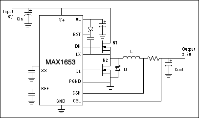 Figure 1. This illustrative step-down switching regulator features an externalswitching transistor (N1) and synchronous rectifier (N2).During normal operation, the circuit conducts current from input to output when the high-side switch (N1) is on, and it continues conducting through the inductor when N1 is off and the synchronous rectifier (N2) is on. First-order approximations of the current and voltage waveforms (Figure 2) lead to a flawed assumption that all the components are ideal, but the parasitic effects of these components will be covered later.
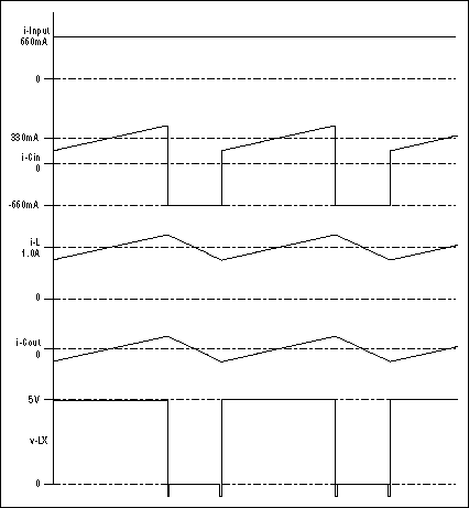 Figure 2. These waveforms from the circuit in Figure 1 are based on an assumption of ideal components.Because N1 is on only part-time, the input source and input capacitor (CIN) see discontinuous currents. CIN supplies the excess current (IL -IINPUT) while N1 is on, and it stores charge from the input current while N1 is off. If CIN were of infinite value, with zero equivalent series resistance (ESR) and equivalent series inductance (ESL), the voltage across it would remain constant during these partial charge and discharge cycles. Actual voltage fluctuates over each cycle, of course. The current pulses divide between CIN and the input source, based on the relative conductance at or above the converter's switching frequency.One way to eliminate these conducted emissions is the brute force approach: Connect low-impedance bypass capacitors at the input. Yet a more subtle approach can save cost and board area: Add impedance between the source and the converter, making sure the necessary DC current can pass. The best impedance is an inductor, but take care that the converter's input impedance remains low up to its loop crossover frequency. (The loop crossover for most DC/DC switching converters is between 10kHz and 100kHz.) Otherwise, input-voltage fluctuations can destabilize the output voltage. Current ripple on the output capacitor (COUT) is much less than on CIN. Its amplitude is lower, and (unlike the input capacitor) its current is continuous, and therefore has less harmonic content. Normally, each turn of the coil is covered with wire insulation, forming a small capacitor between each pair of turns. Adding these parasitic capacitors in series forms a small equivalent capacitor in parallel with the inductor, which provides a path for conduction of current impulses to COUT and the load. Thus, the discontinuous edges of the voltage waveform at the switching node (LX) conduct high-frequency current to COUT and the load. The usual result is spikes on the output voltage, with energy in the 20MHz to 50MHz range. Often the load for this type of converter is some form of microelectronics susceptible to conducted noise, and fortunately the converter's conducted noise is easier to control at the output than at the input. As for the input, output conducted noise can be controlled by very low impedance bypassing or secondary filtering. One should be cautious of secondary (post) filtering, however. Output voltage is a regulated variable in the control loop, so an output filter adds delay or phase (or both) to the loop gain, possibly destabilizing the circuit. If a high-Q LC post-filter is placed after the feedback point, the inductor's resistance will degrade the load regulation, and transient load currents can cause ringing.
Other Topologies
Other switching-converter topologies have problems similar to those of the step-down converter. A step-up converter (Figure 3), for example, has the basic structure of a step-down converter, but with inputs and outputs swapped. Thus, problems at the input of a step-down converter apply to the input of a step-up converter as well, and vice versa. Figure 3. This step-up switching regulator lacks synchronous rectification, but is otherwise similar to the step-down type, with inputs and outputs swapped.Step-down converters are limited, because their output voltage must be less than the input voltage. Similarly, a step-up converter's output voltage must be greater than its input voltage. This requirement is problematic when the output voltage falls within the input-voltage range. A topology that solves this problem is the flyback converter (Figure 4).
 Figure 4. A flyback regulator maintains regulation for inputs that range above and below the output voltage.Because currents at the input and the output are both discontinuous, making conducted emissions more difficult to control, noise from this converter is generally worse than that of a step-up or step-down type. Another problem with this converter is that current in each transformer winding is discontinuous, and these discontinuities act with the transformer's leakage inductance to produce high-frequency spikes, which can conduct to other circuits. Physical separation of the primary and secondary windings causes this leakage inductance. Thus, the leakage inductance results from magnetic fields in the air (because fields in the core couple both the primary and secondary windings). Spikes due to the leakage inductance therefore cause magnetic field radiation. Another topology that solves the problem of overlapping input and output voltages is the single-ended primary inductance converter (SEPIC). Similar to a flyback circuit, the SEPIC converter connects a capacitor between the transformer's primary and secondary windings (Figure 5). This capacitor, which provides a path for current in the primary and secondary windings during the time that flyback currents are off, improves the flyback circuit by making the primary and secondary currents continuous. On the other hand, adding input or output capacitance to a flyback circuit can often improve its emissions sufficiently to make that topology just as acceptable. If conducted and radiated noise is expected to be a problem, however, the SEPIC circuit can be preferable to the flyback.
 Figure 5. Otherwise similar to a flyback regulator, the single-ended primary inductance converter (SEPIC) has continuous primary and secondary currents that generate less noise.
Linear Post-Regulation
For some applications in which output noise must be minimized, the efficiency deficit of using a linear regulator is not acceptable. A switching regulator followed by a linear post-regulator can be suitable in these cases. The post-regulator attenuates high-frequency noise generated by the switching regulator, resulting in noise performance approaching that of a lone linear regulator. Because most voltage conversion occurs in the switching regulator, however, the efficiency penalty is much smaller than for a lone linear regulator.This scheme can also replace flyback and SEPIC converters in applications for which the input and output voltages overlap. The step-up converter operates when the input is less than the output, and the linear regulator operates when the input is greater than the output. A step-up converter and a low dropout (LDO) linear regulator can be combined in a single IC (Figure 6). This device also includes a track mode in which the step-up converter output voltage is always 300mV above the LDO output voltage. As a result, the LDO regulator maintains sufficient PSRR and headroom (input minus output voltage) to attenuate noise from the step-up converter under all conditions. Figure 6. As a third option for maintaining regulation when the input range overlaps the output voltage, this IC combines a switching regulator (for step up) and a linear regulator (for step down).
Common-Mode Noise
By definition, common-mode conduction is in phase on both connections of the input or the output. Typically, it poses a problem only for fixed systems that have a path to earth ground. In a typical offline power supply with common-mode filters (Figure 7), the main source of common-mode noise is the MOSFET. The MOSFET is usually a major power-dissipating element in the circuit, and it requires a heatsink.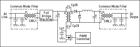 Figure 7. Common-mode filters in this typical offline power supply reduce noise that is common to both sides of the input and the output.For a TO-220 device, the heatsink tab would connect to the MOSFET drain, and in most cases the heatsink would conduct current to earth ground. Because the MOSFET is both insulated and electrically isolated from the heatsink, it has some capacitance to earth ground. As it switches on and off, the rapidly changing drain voltage drives current through the parasitic capacitance (CP1) to earth ground. Because the AC line has low impedance to earth ground, these common-mode currents flow from the AC input to earth ground. The transformer, too, conducts high-frequency current through the parasitic capacitance (CP2A and CP2B) between its isolated primary and secondary windings. Thus, noise can be conducted to the output as well as the input.In Figure 7, the common-mode conducted noise is attenuated by the common-mode low-pass filters between the noise source (the power supply) and the input or the output. Common-mode chokes (CML1 and CML2) are generally wound on a single core with the polarity shown. Load current and the line current driving the power supply are both differential-mode currents (that is, current flowing in one line flows out the other). By winding the common-mode chokes on a single core, the fields due to differential-mode currents cancel, allowing use of a smaller core because very little energy is stored in it.Many of the common-mode chokes designed for offline power supplies are wound with physical separation between the windings. This construction adds differential-mode inductance, which also helps to reduce the conducted differential-mode noise. Because the core links both windings, fields due to differential-mode current and inductance are in the air rather than the core, which can produce radiated emissions.Common-mode noise generated in the power supply's load can be conducted through the power supply to the AC line by means of parasitic capacitance (CP2A and CP2B) in the transformer. A Faraday shield in the transformer (a ground plane between primary and secondary) can reduce this noise (Figure 8). The shield forms capacitors from the primary and secondary to ground, and these capacitors shunt common-mode currents to ground rather than allowing them to pass through the transformer.
 Figure 8. A Faraday shield between primary and secondary blocks common-mode noise that would otherwisepass through the transformer's parasitic interwinding capacitance.Just as conducted emissions can be in the form of voltage or current, radiated emissions can be in the form of electric or magnetic fields. Because fields exist in space rather than in conductors, however, there is no distinction between differential-mode and common-mode fields. An electric field exists in the space between two potentials, and a magnetic field exists around a current traveling through space. Both fields can exist in a circuit, because capacitors store energy in electric fields and inductors/transformers store/couple energy in magnetic fields.
Electric Fields
Because an electric field exists between two surfaces or volumes with different potentials, it is relatively easy to contain the electric field noise generated within a device by surrounding the device with a ground shield. Such shielding is common practice in the construction of CRTs, oscilloscopes, switching power supplies, and other devices with fluctuating high voltages. Another common practice is the use of ground planes on circuit boards. Electric fields are proportional to the potential difference between surfaces and inversely proportional to the distance between them. They exist, for instance, between a source and any nearby ground plane. Multilayer circuit boards therefore let you shield circuitry or traces by placing a ground plane between them and any large potential.Yet one should be cautious of capacitive loading on high-voltage lines when using ground planes. Capacitors store energy in electric fields, so placing the ground plane near a conductor forms a capacitor between the conductor and ground. A large dV/dt signal on the conductor can cause large conducted currents to ground, thereby degrading the conducted emissions while controlling the radiated emissions.If electric field emissions are present, the most likely culprit is the highest potential in the system. In power supplies and switching regulators, beware of the switching transistors and rectifiers, because they normally have high potentials and can also have large surface areas due to heatsinking. Surface-mount devices can have this problem, too, as they often require lots of circuit-board copper for heatsinking. In that case, also watch out for capacitance between any large-area heatsink plane and the ground plane or a power-supply plane.Magnetic Fields
Electric fields are relatively easy to contain, but magnetic fields are a different proposition. Enclosing a circuit in high-µ material can provide an effective shield, but that approach is difficult and costly. Usually the best way to control magnetic field emissions is to minimize them at the source. In general, this requires that you choose inductors and transformers designed to minimize radiated magnetic fields. What is equally important is for the circuit-board layout and interconnect wiring to be configured to minimize the size of current loops, especially in high-current paths. Not only do high-current loops radiate magnetic fields, but they also increase the inductance of conductors, which can cause voltage spikes on lines that carry high-frequency current.Inductors
Circuit designers not experienced in transformer or inductor design are likely to choose off-the-shelf transformers and inductors. Even so, a bit of knowledge about magnetics can enable a designer to select the optimal components for an application.The key to reducing inductor emissions is using high-µ material for keeping the field in the core and out of the surrounding space. Magnetic fields have a proportionally higher density in higher-µ material. This is much like parallel conductance: A 1S conductance (i.e., a 1Ω resistor) in parallel with a 1mS conductor (1kΩ resistor) has 1000 times' the current of the 1mS conductor. A magnetic field density divides in a ratio of 1000:1 between a 1000µ, 1in² core and a 1µ, 1in² core. High-µ materials cannot store a lot of energy, so for compact inductors one must employ a high-µ core with an air gap.To understand why, look at Figure 9. The B-field (X-axis) is proportional to V×t/N, where N is the number of turns. The H-field (Y-axis) is proportional to N×i. Thus, the slope of the curve (proportional to µ) is also proportional to the inductance (L = V/[di/dt]). Adding a gap to this ferrite (or any other high-µ core) reduces the slope, thereby lowering the effective µ and consequently the inductance. Inductance decreases by the change in slope, maximum current increases by the change in slope, and the saturation B-field remains the same. Therefore, the maximum energy (½LI²) stored in the inductor increases. This increase can also be illustrated by applying a voltage to the inductor and noting the amount of time to reach Bsat. Energy stored in the core is the integral of (V×i)dt. Because the current associated with a gapped core is higher for the same voltage and time, the corresponding level of stored energy is higher. Figure 9. Gapping a ferrite core forces magnetic flux out of the core and allows the inductor or transformer to store energy in a field surrounding the device.Gapping the core, however, increases magnetic field radiation in the space around the inductor. Bobbin cores, for example, whose large air gap makes them notorious generators of magnetic field radiation, are generally avoided in some noise-sensitive applications for that reason. The bobbin core, which is just a bobbin-shaped piece of ferrite, is one of the simplest and cheapest types of gapped ferrite core. Wire is wound around the center post to make an inductor. Costs are low because the wire can be wound directly around the core with no extra work other than terminating the wire. In some cases the wires are terminated on a metallized area at the bottom of the core, allowing the inductor to be surface-mounted. In other surface-mounted components, the inductor is mounted on a ceramic or plastic header, to which the wires are terminated.Some manufacturers put ferrite shields around the bobbin core to help reduce field emissions. This measure helps, but it also reduces the gap and therefore decreases the energy that can be stored in the core. Because the ferrite itself can store very little energy, a small gap is often retained between the shield and the core, which allows some unwanted radiation of magnetic fields in this type of inductor. Depending on the level of acceptable emissions, however, the bobbin core can be a good compromise between cost and EMI.Various other core shapes can be gapped (or not) according to the requirements of the application. Pot cores, E-I cores, and E-E cores, for example, all have center legs or posts that can be gapped (Figure 10). Gapping the center of the core, which is completely surrounded by the coil, helps to reduce the emissions radiated from the air gap. These inductors are usually more expensive, because the coil must be wound separately from the core, and the core parts assembled around the coil. For easy design and assembly, cores can be purchased with a pregapped center leg.
 Figure 10. Different core geometries offer trade-off among energy storage, field emission, and ease of assembly. All can be gapped.Perhaps the best core for reducing radiated emissions is the distributed-gap toroid. This core is made by pressing a mixture of filler and high-µ metal powder into the doughnut shape of a toroid. The grains of metal powder, separated by nonmagnetic filler, have small air gaps between them that create an overall "air gap" distributed evenly throughout the core. The coil is wound through the center and around the outside of this core, making the field travel in a circle along the middle of the coil. As long as the coil is wound around the whole circumference of the toroid, it shields the outside by surrounding the magnetic field completely.The loss in a typical distributed-gap toroidal core is sometimes higher than for gapped ferrites, because metal grains in the toroid are susceptible to eddy currents that generate heat and reduce power-supply efficiency. Toroids are also expensive to wind, because wire must be fed through the center of the core. Machines can do this, but they are slower and more expensive than traditional coil-winding machines. Some ferrite toroidal cores have a discrete air gap. The resulting magnetic field emissions are higher than those of distributed-gap cores. Yet typical gapped toroids have lower losses, because they contain the field better than other discretely gapped ferrite cores. The coil reduces emission by shielding the gap, and the toroidal shape helps to keep the field inside the core.
Transformers
Transformers have many limitations in common with inductors, because they are wound on the same cores. Some issues are unique to transformers, however. The performance of actual transformers can approach that of an ideal transformer— coupling voltage from primary to secondary with a ratio of voltages proportional to the ratio of turns in each winding.The equivalent circuit of a transformer (Figure 11) models the interwinding capacitance as CWA and CWB. The problem posed by these parameters is mainly that of common-mode emissions in isolated power supplies. Winding capacitances CP and CS are small and usually negligible at the operating frequencies of switching power supplies and regulators. The magnetizing inductance LM is important, because too much magnetizing current can cause the transformer to saturate. As for inductors, saturation increases the magnetic field emission from the transformers. Saturation also causes higher core loss, higher temperature (with the possibility of thermal runaway), and a degradation of coupling between the windings. Figure 11. Parasitic elements in the equivalent model for a transformer modify its ideal behavior.Leakage inductance is caused by a magnetic field that links one winding but not the other. Though some coupled inductors and transformers (like the common-mode choke discussed earlier) are designed for a high level of this parameter, leakage inductances LLP and LLS are the most problematic parasitic elements in a switching power supply. Magnetic flux that links two windings couples those windings together. All transformer windings are around the core, so any leakage inductance is outside the core, in the air, where it can cause magnetic field emissions.Another problem with leakage inductance is the large voltage generated when the current changes quickly, as it does in the transformer of most switching power supplies. Such voltage can overstress the switching transistor or rectifier. Dissipative snubbers (usually a series resistor and capacitor) are often used to control this voltage by dissipating the energy of the voltage spike. On the other hand, some switching devices are designed to withstand repetitive avalanche breakdowns and can dissipate the energy without external snubbers.The leakage inductance of a transformer can be determined by shorting the secondary and measuring the inductance at the primary. This measurement includes any secondary leakage inductance coupled through the transformer, but in most cases such leakage must be accounted for anyway because it adds to the primary voltage spike. The corresponding spike energy is calculated as E = ½LI², so power lost to the leakage inductance is the energy of each spike multiplied by the switching frequency: P = ½LI²f.Transformer requirements depend on the power-supply topology. Topologies that couple energy directly across the transformer, such as half-bridge, full-bridge, push-pull, or forward converters, require a very high magnetizing inductance to prevent saturation. The transformer's primary and secondary simultaneously conduct current in these circuits, coupling the energy directly through the transformer. Because little energy is stored in the core, the transformer can be smaller. These transformers are wound typically on an ungapped core of ferrite or other high-µ material.Other power-supply topologies require that the transformer core store energy. The transformer in a flyback circuit stores energy by means of the primary in the first half of the switching cycle. In the second half of the cycle, energy is retrieved and fed to the output by means of the secondary. As is true for inductors, an ungapped high-µ core is not suitable for storing energy in a transformer. Instead, the core must be gapped discretely or have a distributed gap. The resulting component will be larger than one with an equivalent ungapped core, but it can save an extra inductor as well as cost and space.
Layout
Component selection is very important in controlling EMI, but the circuit-board layout and interconnects are equally important. Especially for the high-density, multilayer circuit boards often used in switching power supplies, layout and component placement are critical to the circuit's proper operation and interaction. The power switching can cause large dV/dt and di/dt signals in the circuit-board traces, which lead to compatibility problems by coupling to other traces. Compatibility problems and expensive circuit-board revisions can be avoided, however, by taking extra care in the layout of critical paths.A distinction can be made between radiated and conducted emissions in a system, but the distinction blurs when talking about interference in a circuit board and wiring. Adjacent traces that couple electric fields also conduct currents by means of parasitic capacitance. Likewise, traces that are coupled by magnetic fields act somewhat like transformers. These interactions can be described in terms of lumped components or through field theory. Which approach to take depends on which method more accurately describes the interaction.Crosstalk
Two or more conductors in close proximity are coupled capacitively; therefore, large voltage changes on one will couple currents to the other. If the conductor's impedance is low, the coupled currents generate only small voltages. Capacitance is inversely proportional to the distance between the conductors and proportional to the area of the conductors, so the conducted noise can be minimized by keeping the area of the adjacent conductors small and their separation large. Another method for reducing the coupling between conductors is to add a ground plane or shield. A ground trace (or in some cases a power-supply bus or other low-impedance node) between conductors can prevent their interaction by coupling them capacitively to ground instead of to each other. But exercise caution. Traces carrying fast dV/dt changes, positioned close to a plane with high-impedance interconnect to ground, can couple these changes to the ground plane. In turn, the ground plane can couple the signals to sensitive lines, thereby exacerbating rather than helping the noise problem. If the ground plane doesn't carry large currents, it can be tempting to connect it to ground through a small wire. Yet the high inductance of a small wire can cause the ground plane to look like a high impedance to fast-changing voltages. One must take care to ensure that a ground plane does not inject noise into sensitive parts of a circuit. Input and output bypass capacitors, for example, often pass current through a ground plane, and the high-frequency current components can affect sensitive circuitry. To prevent this problem, circuit boards often include separate planes for the power and signal grounds. Connected at a single point, these planes minimize the noise injected into signal ground by potentials generated across the power-ground plane. This practice is similar to that of a star ground, in which all components connect to ground at a single point (all traces leave that point in a "star" pattern). The star ground has the same effect as separate power- and signal-ground planes, but it isn't practical for large, complex circuit boards including lots of grounded components.If a node is known to be sensitive to injected noise, then traces and wires connected to that node should be routed away from nodes with high-voltage changes. If that isn't possible, add a good ground or a shield. Good capacitive bypassing of the node can also decrease its susceptibility to crosstalk. Normally, a small capacitor connected between the node and ground or between the node and a power-supply bus forms a suitable bypass.When choosing the bypass capacitor, make sure it has low impedance over the range of frequencies that are problematic potentially. Equivalent series resistance (ESR) and equivalent series inductance (ESL) can cause the impedance to be higher than expected at high frequencies, so the low ESR and ESL of ceramic capacitors is attractive for bypass applications. The ceramic dielectric has a major effect on performance as well. Higher-capacitance dielectrics (such as Y5V) can allow large changes in capacitance over voltage and temperature. At maximum-rated voltage, capacitors made with these ceramics can exhibit as little as 15% of their unbiased capacitance. A smaller capacitance value with a better dielectric, yielding crosstalk attenuation that is not as dependent on bias and temperature, will in many cases provide better and more consistent bypassing.The placement of bypass capacitors is also critical. To attenuate high-frequency noise, you must route the signals in question through the bypass capacitor. In Figure 12a, the length of trace in series with the capacitor adds to its ESR and ESL, increasing the impedance at high frequencies and reducing the capacitor's effectiveness as a high-frequency bypass. A better layout routes the trace through the capacitor, so the traces' stray ESR and ESL aid the bypass capacitor's filter action rather than degrading it.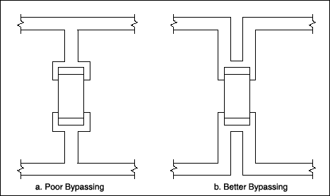 Figure 12. Poor bypass connections (a) add trace better connection (b), trace parasitics add to the capacitor's filter action.Some nodes should not be bypassed, because doing so changes their frequency characteristics. An example is the feedback resistor divider. In most switching power supplies, a resistive feedback divider drops the output voltage down to a level acceptable to the error amplifier. A large bypass capacitor added to this feedback node forms a pole with the resistance of that node. Because the divider is part of the control loop, this pole becomes part of the loop characteristic. If the pole frequency is less than one decade above the crossover frequency, its phase or gain effects can affect the loop stability adversely.
Inductance
Some currents in a switching power supply switch on and off quickly. Stray inductance in those current paths can induce large noise voltages, which couple into sensitive circuitry and stress the components. Lines carrying DC currents seldom lead to problems, because DC does not cause voltage spikes or couple AC to other traces. A line in series with an inductor, for instance, is not a problem, because the stray inductance is much smaller than the inductor value. The large series inductance also prevents discontinuities in the current. If a circuit produces discontinuous currents, try to prevent the current from traveling in large loops. Large loops of current produce larger values of inductance, thereby increasing any consequent magnetic field radiation. This caveat applies to component placements as well, because current usually switches between active devices such as transistors and diodes.Consider the step-down converter in Figure 1. When the high-side MOSFET switch (N1) is on, current travels by means of the input, N1, the inductor, and the load. After N1 turns off, the diode (D) conducts current until the synchronous rectifier (N2) turns on. Current then flows through N2 until it turns off; then the diode carries current until the cycle starts again. Note that currents through the inductor and the output capacitor are continuous, and therefore should not be major contributors to noise. If N1, N2, and D are placed some distance from one another, the surrounding fields must shift quickly, in response to the rapid current changes within them. Because the voltage generated is proportional to the change in the magnetic field with time (dΨ/dt), these rapid field fluctuations can generate large voltage spikes. Note that the input source and the output load carry high-frequency currents. These currents should pass through the input and output bypass capacitors; otherwise, they are conducted through the input or output lines (or both). See the section on conducted emissions. The impedance of input and output bypass capacitors is important. They should be large enough to keep the impedance low at input and output, but larger capacitors (tantalum or electrolytic types, for instance) have higher ESR and ESL than smaller ceramic types. You must therefore ensure that the impedance of the capacitors is sufficiently low at the frequencies of concern.One alternative is to parallel a ceramic capacitor with an electrolytic or tantalum capacitor, because the ceramic capacitor has lower impedance at high frequencies. In most cases, however, that arrangement is no better than multiple electrolytic or tantalum capacitors in parallel to reduce ESR and ESL, or multiple ceramic capacitors in parallel to increase the total capacitance.关于布线技巧与EMC就介绍完了,您有什么想法可以联系小编。